About Me

About Me |
|
Welcome at my web site. My name is Peter Luethi and I live near Zurich, Switzerland. After having finished my Ph.D. study in the field of fourth-generation multiple-input multiple-output (MIMO) wireless communication at the Integrated Systems Laboratory of the Swiss Federal Institute of Technology (ETH Zurich) in Zurich, Switzerland, I work now as R&D and technology consultant for government organizations as well as small to multi-national industrial companies, for instance in the medical technology sector. Before pursuing my Ph.D. study, I worked for nearly three years at Advanced Micro Devices (AMD) Inc., in Dresden, Germany, and was involved with HyperTransport™ and PCI verification and performance enhancements concerning AMD K8's Southbridge development activities.
Among my favorite hobbies are recreational scuba diving, playing volleyball (body height 2.00m, so do not ask on which position...), hiking in the swiss mountains, cycling, creating convenient electronic circuits and building and building and building and finally flying radio-controlled model airplanes. Take a glance at one of my "babies": Super Stearman, Nomad,...
I hope this web site provides you some inspiration, useful information or applications to develop your own electronic circuits.
In 1999, I have been working for three months at Philips Semiconductors Zurich. I have updated and built new cell libraries (Cadence PCells) for the Cadence Design Framework. I was involved with creating Parameterizable on-chip CMOS decoupling Capacitors and Parameterizable high-voltage CMOS Transistors (0 - 16 V). The aim of my project was to get easy drag and drop cells with automatic DRC-compliant layout generation, so that the analog design engineers do not have to draw (and match) the layout all the time by hand. The silicon technology was a single poly, 2 metal, 0.6um CMOS process. These parameterizable cells were used in CMOS LCD driver chips for mobile phones. At that time, these LCD driver chips were sold as ASSPs (application specific standard product) and were used in almost every Nokia mobile with monochrome LCD display.
During my study at the ETH Zurich, I have also participated in a robot engineering contest. Our team consisted of 5 students; 3 electrical engineers and 2 mechanical engineers. In short, the task was to design an autonomous navigating and mail-collecting robot. In the end, we managed to achieve 3rd place in the final live contest. Here are some pictures of the Swiss SmartROB Championships 1999.
I also participated in a student project called "Parameterizable Hybrid Stack-Register Processor as VHDL Soft Intellectual Property Module". The task was to design a processor for a specific network application, which required to handle medium to high interrupt rates very efficiently. Therefore our processor architecture was based on a mixture between stack and register-based architecture to incorporate the advantages of both of them. The corresponding research paper was finally presented at the 13th Annual IEEE International ASIC/SOC Conference in Washington D.C., USA.
The second student project, a "Low-Cost Inertial Navigation System", intended to build and assess an inertial navigation platform consisting entirely of cost-effective solid-state sensors such as piezo-based acceleration sensors and piezo-based gyros. The aim was to characterize the precision of such an inertial navigation system (INS) and to identify possible bottlenecks, specific issues, or general drawbacks. The entire platform consisted of three acceleration sensors, three gyros, some analog filter circuitry, a PCMCIA data acquisition card, and a portable computer. In the end, it worked quite well: The setup was suitable for measuring and controlling the spatial representation of the system, i.e., the current acceleration and angular orientation, but was not able to track the actual position accurately. First, the accuracy of the solid-state sensors has to be improved by at least a factor of 10 in order to be able to compute a position reliably. Moreover, some sophisticated algorithms like Kalman filters and adequate position feedback/update mechanisms need to be applied, maybe in conjunction with additional GPS data.
During my spare time, I was also engaged with designing a precision digital altimeter consisting of the Motorola MPXS4100A absolute pressure sensor, the NSC ADC12130 12-bit A/D converter, two PIC 16F84 microcontroller, a dot-matrix LCD display, and a wireless transmitter and receiver. The intention was to get the actual altitude of my airplanes in real-time and providing the base hardware setup for further ideas such as a variometer. However, time was limited and today, there exist already various commercial solutions...
In late 2000, my master's thesis in electrical engineering dealt with the performance characterization of the prototype Southbridge for the chipset of the AMD 64-bit "hammer series" processors (the powerful "Sledgehammer" and his smaller counterpart, the "Clawhammer") at AMD Dresden Design Center, in Dresden, Germany.
 |
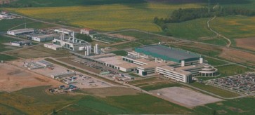 |
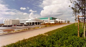
| AMD Fab 30 Saxony, Dresden, Germany (historic pictures, around the year 2000) | |
The task was to setup a Southbridge performance analysis environment being capable of revealing possible performance bottlenecks already during design time and providing corresponding suggestions for performance enhancements. The performance analysis should cover the entire Southbridge with all its specific bus protocols, and at that time, also the new Lightning Data Transport (LDT) bus, now officially known as HyperTransport™ (HT). The LDT bus, developed and standardized by a special interest group including AMD, was implemented between North- and Southbridge and served for instance the 64-bit/66 MHz PCI bus bridges and the peripheral devices attached to the Southbridge.
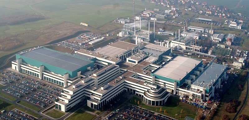 |
| AMD Fab 36 Saxony, Dresden, Germany (around the year 2006, now acquired by GlobalFoundries) |
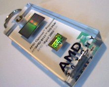
I have been working at the AMD Dresden Design Center, Dresden, Germany from 2001 to 2003 on RTL-based block- and system-level verification and performance analysis for next-generation HyperTransport™ chipsets for AMDs x86-64 CPUs (see picture of AMD 8111 x86-64 Southbridge "Thor" below). My task was to ensure the correct functionality and interoperability of several HyperTransport™ Southbridges for AMD's K8 CPUs. I received the "AMD Fab 30 Vice President's Award" for outstanding achievements in conjunction with my diploma thesis "Performance Analysis of AMD Southbridge Zorak". In March 2003, I received the best presentation award from the audience at "Verisity's Club Verification" for "Verification Glue: How to compose System-Level Environments", introducing the verification concept having been employed for Southbridge verification.
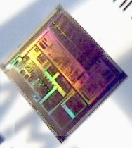
AMD x86-64 CPU "Hammer" |
AMD x86-64 Server Setup |
AMD 8111 x86-64 Southbridge "Thor" |
After having been abroad for nearly 3 years, I moved back from Dresden, Germany to Zurich, Switzerland in September 2003 in order to start a Ph.D. study back at the Integrated Systems Laboratory of the ETH Zurich in Zurich, Switzerland. My research project was about specific circuits and systems for fourth-generation multiple-input multiple-output (MIMO) wireless communication systems. The main objectives of MIMO technology are a significant increase in throughput, range and/or quality of service (QoS) by using the same channel bandwidth and transmit power expenditure as traditional wireless communication systems. As major innovation, MIMO technology additionally exploits the spatial dimension such as to transmit multiple data streams simultaneously and in the same frequency band.
Nevertheless, MIMO-based wireless communication can only deliver on its promises, if there exists a so-called rich-scattering environment, i.e. numerous signal reflections are present at the receiver, for instance in a large open indoor office environment. Radio signals which are traveling across such an environment get their individual spatial signature imposed by different wave reflections and absorptions. In general, these spatial signatures are affected by the frequency of the signal, the propagation environment (channel), but very important, also by the individual locations of transmit and receive antennas.
Using MIMO communication schemes, we transmit different (independent) data streams from spatially different transmit antennas to spatially different receive antennas, therefore every received signal ideally obtains its independent spatial signature. Since all radio signals are transmitted simultaneously and in the same frequency band, the receiver gets a superposition of all signals. The task of the MIMO receiver is to separate this superposition of signals into different (independent) data streams. Basically, the individual spatial signatures can be acquired and measured in the receiver (channel estimation), and afterwards prepared for compensation (channel inversion). The subsequent equalization of the received signal intends to split the received signal into different data streams originally sent by the MIMO transmitter. The complexity and performance of channel inversion and data equalization are heavily depending on the underlying MIMO detection algorithm. Unfortunately, the benefits of MIMO technology come at the expense of a significantly increased signal processing complexity. Therefore, sophisticated algorithms and high-performance digital integrated circuits are the prerequisites for successful leverage of this promising wireless communication technology.
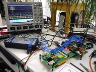
My research activities started with algorithm analysis and assessment in MATLAB, i.e., selection of suitable candidate algorithms with respect to adequate algorithmic performance, suitability for hardware implementation, susceptibility for reduced-precision effects concerning fixed-point implementation, and VLSI implementation aspects such as hardware complexity and computational throughput, for instance. After thorough MATLAB assessment, my research activities continued with hardware-specific algorithmic optimizations, VHDL coding of a subset of algorithms, functional verification, RTL synthesis and physical integration as ASIC, followed by testbed deployment of the manufactured ASIC using a custom-built PCB.
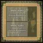
MMSE-SQRD ASIC |
Socket for MMSE-SQRD ASIC |
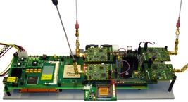
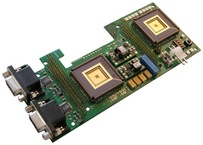
Embedded real-time 4x4 MIMO-OFDM testbed |
MMSE-SQRD ASIC deployment |
In the end, selected ASICs proved flawless operation in a FPGA-based 4x4 MIMO prototyping platform under real-time constraints and real-world conditions and therefore successfully demonstrated the feasibility and applicability of specific MIMO preprocessing schemes for practical wireless communication systems. Finally, my Ph.D. thesis aims at providing reference figures for throughput and silicon complexity of selected MIMO preprocessing algorithms, and thus seeks to serve as a basis for possible future highly-integrated commercial 4x4 MIMO communication solutions.

Last update: 2011/08/07