Standard Controller for Dot Matrix LCDs
Terminology
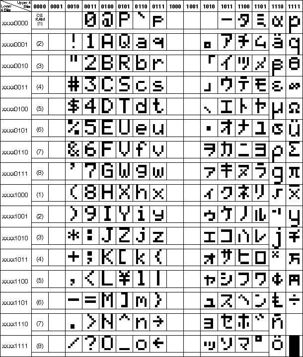
Correspondence between Character Codes
and Character Patterns
Relationship between CGRAM Addresses, Character
Codes (DDRAM) and Character Patterns (CGRAM Data)
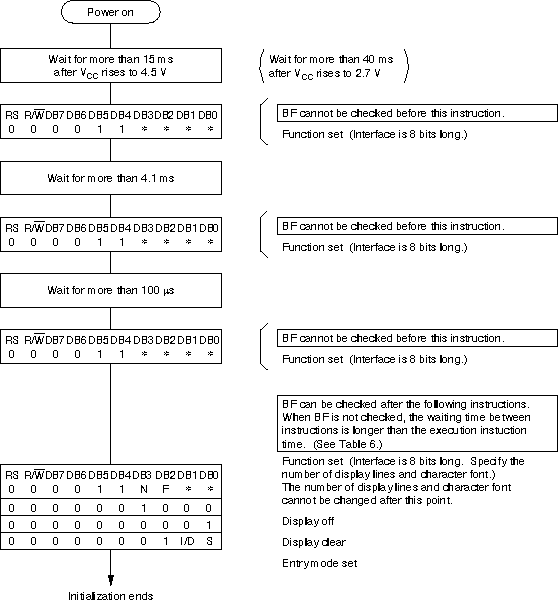
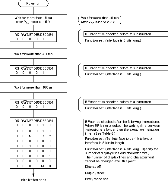
Initializing the LCD by
Instruction
8 bit
Interface
4 bit
Interface
This is only a short reference for the most important commands
not mentionned
in "The Extended Concise
LCD Data Sheet".
| CGROM | Character Generator
ROM Consist of the fix implemented character set (ROM). Character set may differ with different ROM Codes. To display a char, the CGROM address of the character to be showed at the current DDRAM address has to be transmitted to the display. |
| CGRAM | Character Generator
RAM The user-defined character set. With 5x7 dots, 8 character patterns can be written and with 5x10 dots, 4 types can be written. Also reprogrammable during use. To display a char, the CGRAM address of the character to be showed at the current DDRAM address has to be transmitted to the display. |
| DDRAM | Display Data RAM Here is the data stored, which is currently showed on the display (memory mapped I/O). |
| CGRAM-/ CGROM- Address |
The addresses of the characters
patterns in the CGRAM / CGROM. Length : 8 bit |
| DDRAM- Address |
The address of the (maybe
invisible) cursor, where the next char is written to. You can write to all of these addresses (if implemented in silicon), even if they are not actually displayed. So you can store external data on hidden positions. Or you can first write data to the visible and hidden locations and then scroll the whole display to the hidden positions. Length : 8 bit Range: 0x00 - 0x27, 0x40 - 0x67, (...) |
Note: The user can specify any pattern for character-generator RAM (8 different characters).
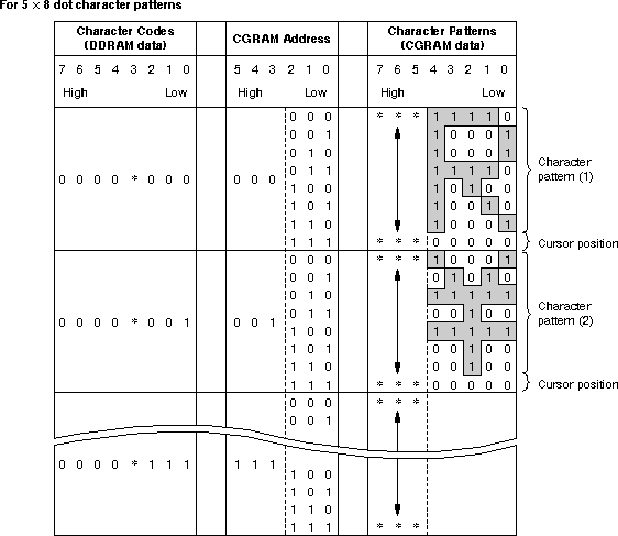
1. Character code bits 0 to 2 correspond to CGRAM address bits
3 to 5 (3 bits: 8 types).
2. CGRAM address bits 0 to 2 designate the character pattern line
position. The 8th line is the
cursor position and its display is formed
by a logical OR with the cursor.
3. Character pattern row positions correspond to CGRAM data bits
0 to 4 (bit 4 being at the left).
4. As shown Table 5, CGRAM character patterns are selected when
character code bits 4 to 7
are all 0. However, since character code
bit 3 has no effect, the R display example above
can be selected by either character code
00H or 08H.
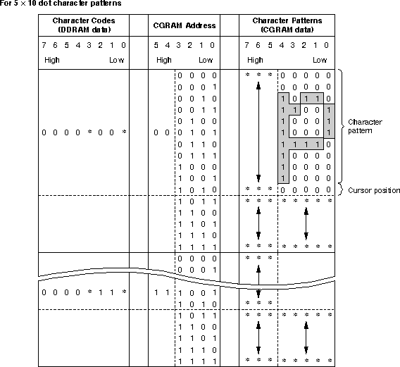
1. Character code bits 1 and 2 correspond to CGRAM address
bits 4 and 5 (2 bits: 4 types).
2. CGRAM address bits 0 to 3 designate the character pattern line
position. The 11th line
is the cursor position and its display is
formed by a logical OR with the cursor.
Since lines 12 to 16 are not used for
display, they can be used for general data RAM.
3. Character pattern row positions are the same as 5 X 8 dot
character pattern positions.
4. CGRAM character patterns are selected when character code bits
4 to 7 are all 0.
However, since character code bits 0 and
3 have no effect, the P display
example above can be selected by
character codes 00H, 01H, 08H, and 09H.
If the power supply conditions for correctly operating the
internal reset circuit are not met,
initialization by instructions becomes necessary.
This procedure must take place in a software reset on a 4 bit
Interface
to assure proper re-entry to the LCD communication.
Refer to the initialization procedure of my LCD
assembler module files, e.g. m_lcd.asm.
Last updated: 2004/12/31